
NVIDIA Co-Packaged Optics Platform: Architecture and Ecosystem
Sources: https://developer.nvidia.com/blog/how-industry-collaboration-fosters-nvidia-co-packaged-optics, https://developer.nvidia.com/blog/how-industry-collaboration-fosters-nvidia-co-packaged-optics/, NVIDIA Dev Blog
Overview
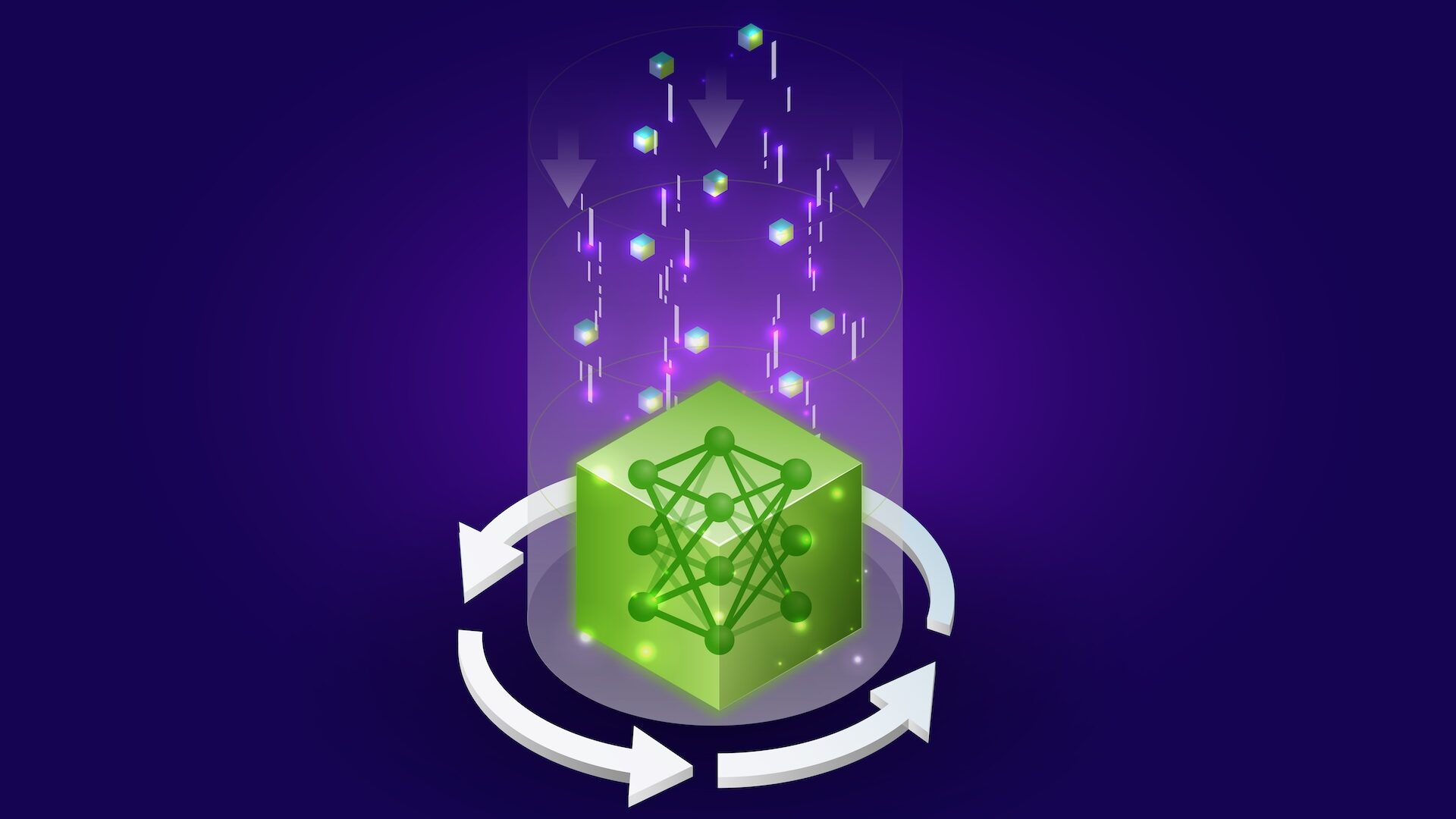
NVIDIA is reshaping data-center connectivity by integrating optical and electrical components, and it does so through close collaboration with industry partners. The NVIDIA networking platform brings together technologies from leaders specializing in advanced foundry processes, cutting-edge lasers, and fiber-to-chip solutions. By coordinating each aspect of the solution design, NVIDIA leverages world-class hardware and supporting capabilities essential for scalable, reliable, and high-performance optical systems. The result is a cohesive ecosystem that addresses growing data throughput needs and energy-efficient design, setting a new standard for optical interconnects. This exploration covers the innovation, partnerships, and technical foundations behind the NVIDIA co-packaged optics (CPO) platform: photonics ICs, electronic ICs, fiber, packaging, connectors, and lasers. The discussion centers on how the NVIDIA ecosystem enables scalable, energy-efficient AI factory interconnects. At the heart of CPO innovation lies the NVIDIA Micro Ring Modulator silicon photonics engine—a breakthrough that redefines density and efficiency for optical interconnects. Engineered for direct 200Gbps PAM4 modulation per wavelength, the Micro Ring Modulator delivers an ultra-low density footprint, enabling unprecedented data throughput without increasing the package size. This level of integration is pivotal for the emerging generation of data-center switches and processors that demand smaller form-factors to minimize power and maximize thermal manageability. Deep collaboration with TSMC has helped NVIDIA address longstanding manufacturing challenges associated with Micro Ring Modulators at production scale. Through advanced process engineering and refined control techniques, NVIDIA and TSMC achieve reliable, repeatable performance even at the smallest geometries, ensuring each modulator meets the exacting standards required for hyperscale deployment. What sets the Micro Ring Modulator apart is its small footprint coupled with robust thermal control. This combination enables multi-row scaling of optical interconnect throughput within a single package, upending traditional floorplan constraints posed by bulkier modulators and enabling dense arrays of high-speed interconnects without compromising power or thermal budgets. When electro-optical interconnects are engineered in tandem, parasitic losses are minimized, and stacked CMOS and photonics components within microns of each other enable ultra-dense, efficient integration. This reduces power consumption and supports compact, thermally manageable modules suitable for hyperscale data centers. Wafer-level integration of micro-lenses reduces both alignment time and sensitivity, streamlining production and enabling scalable wafer-scale manufacturing of high-performance photonics modules. The Quantum-X Photonics switch is powered by a sophisticated optical subassembly designed to deliver unprecedented bandwidth and connectivity for next-generation data centers. Each optical subassembly provides 4.8 Tbps of transmit and 4.8 Tbps of receive bandwidth, anchored by three COUPE-based optical engines, each supporting 1.6 Tbps transmit and 1.6 Tbps receive throughput. Each engine uses eight 200Gbps PAM4 transmit and eight 200Gbps PAM4 receive lanes, with two laser input fibers per engine and eight transmit and eight receive lines. This architecture enables low-latency, high-throughput communication between the switch fabric and its optical interfaces, aligning with the needs of AI-driven and hyperscale environments. A socket-based design for modular connectivity from the electrical interface to the main switch package, together with a hermetically sealed fiber interface to the optical engines, supports rapid deployment and long-term reliability in field conditions. The quantum-scale capabilities are backed by a switch ASIC delivering 28.8Tbps full-duplex bandwidth, using six high-capacity optical subassemblies integrated on the switch package’s interposer to enable dense electrical and thermal coupling and efficient liquid cooling for both the switch core and all optical modules. The Quantum-X Photonics liquid-cooled switch system—Q3450, featuring four Quantum-X chips—provides 115.2Tbps full-duplex bandwidth over 144 ports with 800Gbps per port, supporting low latency and scalable growth for NVIDIA AI factories. The Spectrum-X Ethernet Photonics module package offers the most dense electro-optical packaging yet, integrating 32 silicon photonics engines in a single, compact footprint. Each optical engine is designed with 16 transmit and 16 receive lanes, delivering 3.2Tbps per engine. Together, they enable unprecedented aggregate bandwidth, with 512 lanes of 200Gbps electrical throughput in a compact form factor. The engines are solder-reflown directly onto the module substrate to ensure robust electrical contact and reliability at manufacturing scale. The design includes a detachable optical connector to enable fully automated, mass-manufacturing workflows, simplifying fiber attachment while preserving precision and repeatability. The Quantum-X Photonics and Spectrum-X Ethernet Photonics platforms are powered by an advanced external laser source (ELS) module—a high-power, field-replaceable unit housed in its own thermally controlled environment separate from the main switch chassis. The ELS stabilizes laser operation, reducing wavelength drift and mitigating aging mechanisms caused by thermal cycling. NVIDIA’s adoption of high-power ELS modules centralizes light generation, reducing the total number of lasers in the data center by about a factor of four compared to legacy designs. Each ELS module contains eight lasers precisely coupled via fiber to the optical engines and can power 32 of the Quantum-X switch’s 576 transmit lanes. Spectrum-X Ethernet Photonics uses the same ELS approach, with 16 modules for the single-ASIC version and 64 modules for the quad-ASIC version. The co-packaged solutions for Quantum-X Photonics and Spectrum-X Ethernet Photonics reflect years of NVIDIA-led innovation in collaboration with ecosystem partners. These platforms address challenges at the silicon and transistor levels, as well as thermal management, reliability, high-volume fiber integration with the chip, and consistent laser performance. By blending modularity, efficiency, and robust engineering, they enable data centers to scale to meet the exponential demands of AI-driven applications. For more details, the article references a previous CPO technical blog and a video deep dive into co-packaged optics switches. NVIDIA also directs readers to its silicon photonics site for ongoing announcements and product-release updates.
Key features
- Industry-wide collaboration across foundry, lasers, and fiber-to-chip technologies integrated into a unified NVIDIA networking platform.
- Micro Ring Modulator silicon photonics engine with direct 200Gbps PAM4 modulation per wavelength and ultra-low footprint.
- Production-scale collaboration with TSMC to achieve precise fabrication control, reduced thermal sensitivity, and reliable high-speed modulation.
- Ultra-dense, thermally manageable integration through stacked CMOS and photonics components with minimized parasitics.
- Wafer-level micro-lens integration to streamline fiber alignment and enable scalable manufacturing.
- Quantum-X Photonics switch: 4.8Tbps TX and 4.8Tbps RX per optical subassembly; three COUPE-based engines per subassembly (1.6Tbps TX/1.6Tbps RX per engine); eight 200Gbps PAM4 lanes per engine; modular socket-based subassembly with hermetically sealed fiber interface; six subassemblies per Quantum-X switch ASIC for 28.8Tbps full duplex; Q3450 system delivers 115.2Tbps over 144 ports with 800Gbps per port; liquid cooling in the interposer.
- Spectrum-X Ethernet Photonics: 32 silicon photonics engines, 3.2Tbps per engine, 512 200Gbps electrical lanes; engines solder-reflown onto module substrate; detachable optical connector enabling automated manufacturing with high yield.
- External Laser Source (ELS): high-power, field-replaceable module in a separate thermal environment; eight lasers per ELS; centralizes light generation to reduce laser count by ~4x; powers 32 of the Quantum-X switch’s 576 transmit lanes; 16 ELS modules for single-ASIC and 64 for quad-ASIC Spectrum-X versions.
- Centralized, modular architecture designed for reliability, laser performance consistency, and scalable AI-ready data-center interconnects.
- Practical ecosystem approach that extends across technology, manufacturing, and deployment, with ongoing updates via NVIDIA’s silicon photonics site and related channels.
Common use cases
- AI factories and hyperscale data centers requiring ultra-high bandwidth and energy-efficient interconnects.
- Dense switch fabrics powering next-generation AI compute environments.
- Data-center interconnects that pair high throughput with robust thermal management and reliability.
- Deployment scenarios where modularity and field replaceability (ELS, connectors) improve maintenance and uptime.
Setup & installation
# Setup and installation details are not provided in the source.Quick start
Note: The source does not provide runnable setup or code examples. The following is a high-level architectural outline based on the described platform:
- Review ecosystem partnerships (foundry, lasers, fiber-to-chip) and integration points.
- Assess modular subassemblies (Quantum-X and Spectrum-X) and their interconnects with the main switch package.
- Plan laser-light distribution strategy via the External Laser Source (ELS) modules to minimize laser count and maximize reliability.
- Consider thermal management approaches (liquid cooling, dedicated ELS environments) for long-term reliability.
- Investigate wafer-level photonics integration and hermetically sealed fiber interfaces to support scalable manufacturing.
Pros and cons
- Pros
- Very high density and throughput from Micro Ring Modulator and COUPE-based engines.
- Small footprint enables multi-row scaling and denser packaging.
- Robust thermal control and centralized laser light generation reduce maintenance and laser failures.
- Wafer-level micro-lenses and hermetically sealed interfaces improve alignment speed and reliability.
- Modular, field-replaceable lasers via the ELS reduce onsite maintenance effort.
- External laser modules allow centralized light delivery, reducing the total number of lasers required.
- Cons
- Pricing, licensing, and deployment timelines are not provided in the source.
- The article does not include runnable setup instructions or hands-on deployment steps.
- Real-world field performance and broader adoption timelines are not detailed in the source.
Alternatives
| Approach | Description |
|---|---|
| Legacy non-co-packaged optics | Traditional designs with discrete lasers and separate photonics/electronics modules; higher laser counts and potentially larger footprints. |
| Conventional co-packaged optical subsystems without centralized laser sources | Optics and lasers integrated but without the centralized ELS approach and modular field-replaceability described for Quantum-X Spectrum-X; potentially higher maintenance. |
| Conventional modular photonics without COUPE/TSMC-scale integration | Modules with photonics and electronics not optimized for the same density and thermal performance; may require more space or power per bit. |
Pricing or License
Pricing or licensing details are not explicitly provided in the source.
References
- https://developer.nvidia.com/blog/how-industry-collaboration-fosters-nvidia-co-packaged-optics/
- NVIDIA Dev Blog (co-packaged optics) – referenced materials and product context.
More resources

CUDA Toolkit 13.0 for Jetson Thor: Unified Arm Ecosystem and More
Unified CUDA toolkit for Arm on Jetson Thor with full memory coherence, multi-process GPU sharing, OpenRM/dmabuf interoperability, NUMA support, and better tooling across embedded and server-class targets.

Cut Model Deployment Costs While Keeping Performance With GPU Memory Swap
Leverage GPU memory swap (model hot-swapping) to share GPUs across multiple LLMs, reduce idle GPU costs, and improve autoscaling while meeting SLAs.

Improving GEMM Kernel Auto-Tuning Efficiency with nvMatmulHeuristics in CUTLASS 4.2
Introduces nvMatmulHeuristics to quickly select a small set of high-potential GEMM kernel configurations for CUTLASS 4.2, drastically reducing auto-tuning time while approaching exhaustive-search performance.
Fine-Tuning gpt-oss for Accuracy and Performance with Quantization Aware Training
Guide to fine-tuning gpt-oss with SFT + QAT to recover FP4 accuracy while preserving efficiency, including upcasting to BF16, MXFP4, NVFP4, and deployment with TensorRT-LLM.
How Small Language Models Are Key to Scalable Agentic AI
Explores how small language models enable cost-effective, flexible agentic AI alongside LLMs, with NVIDIA NeMo and Nemotron Nano 2.
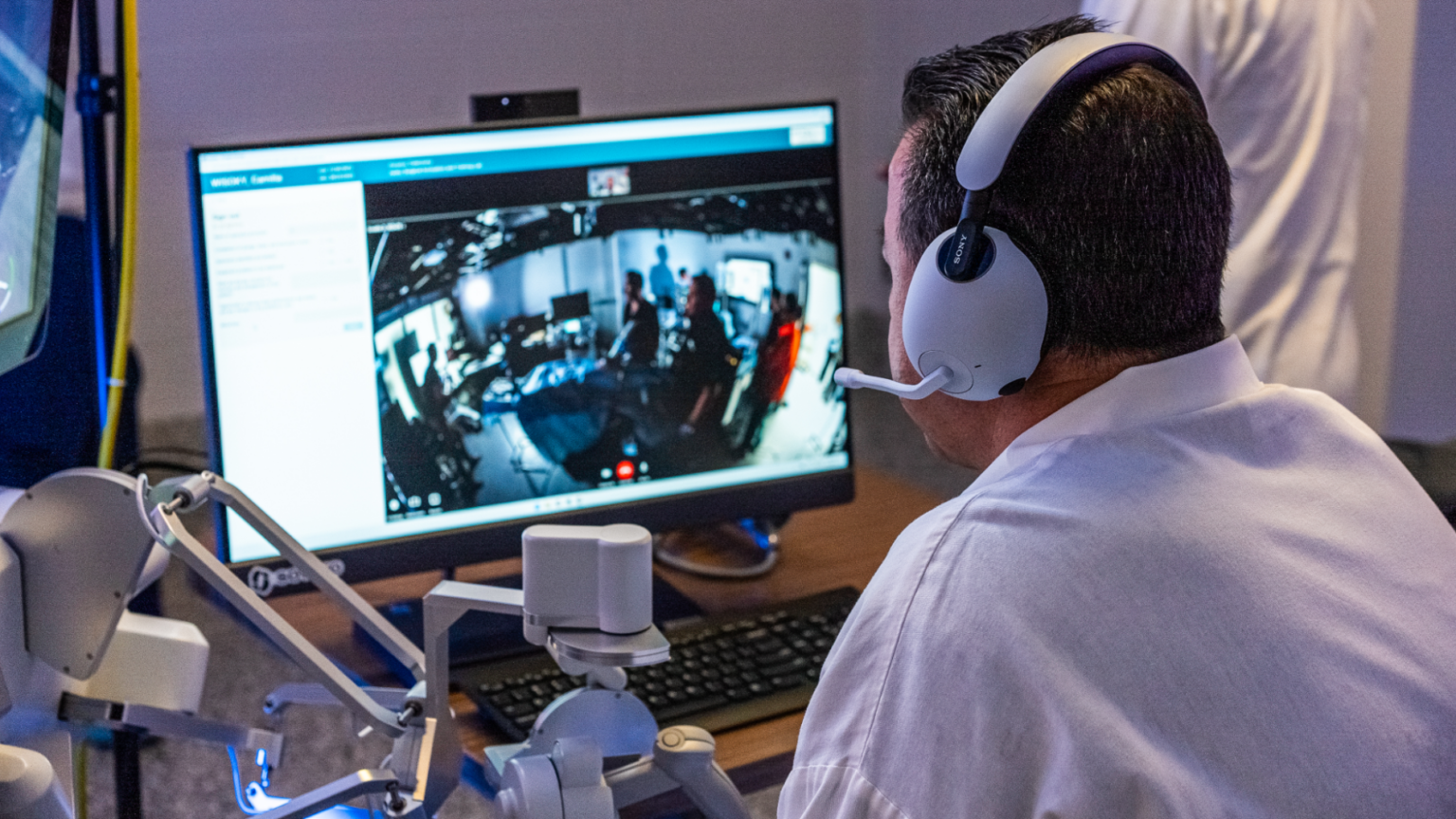
Getting Started with NVIDIA Isaac for Healthcare Using the Telesurgery Workflow
A production-ready, modular telesurgery workflow from NVIDIA Isaac for Healthcare unifies simulation and clinical deployment across a low-latency, three-computer architecture. It covers video/sensor streaming, robot control, haptics, and simulation to support training and remote procedures.