Inside NVIDIA Blackwell Ultra: The Chip Powering the AI Factory Era
Sources: https://developer.nvidia.com/blog/inside-nvidia-blackwell-ultra-the-chip-powering-the-ai-factory-era, https://developer.nvidia.com/blog/inside-nvidia-blackwell-ultra-the-chip-powering-the-ai-factory-era/, NVIDIA Dev Blog
TL;DR
- NVIDIA Blackwell Ultra is the latest member of the Blackwell architecture, engineered for AI factory-scale training and real-time AI services.
- It uses a dual-die design connected by NV-HBI, delivering 10 TB/s bandwidth and enabling a dense, CUDA-programmed accelerator with 208B transistors on TSMC 4NP.
- The GPU features 160 Streaming Multiprocessors (SMs) with four Tensor Cores per SM (640 total), 256 KB TMEM per SM, and the new NVFP4 4-bit precision for substantial efficiency gains.
- Blackwell Ultra delivers up to 15 petaFLOPS NVFP4 performance, 288 GB of HBM3e per GPU, 1 TB unified memory, and enhanced attention processing for large-context models.
- For data-center deployments, Blackwell Ultra supports NVLink (GPU-to-GPU), NVLink-C2C (Grace CPU interop), and PCIe Gen 6 x16, with ConnectX-8 networking to enable AI factories at scale.
Context and background
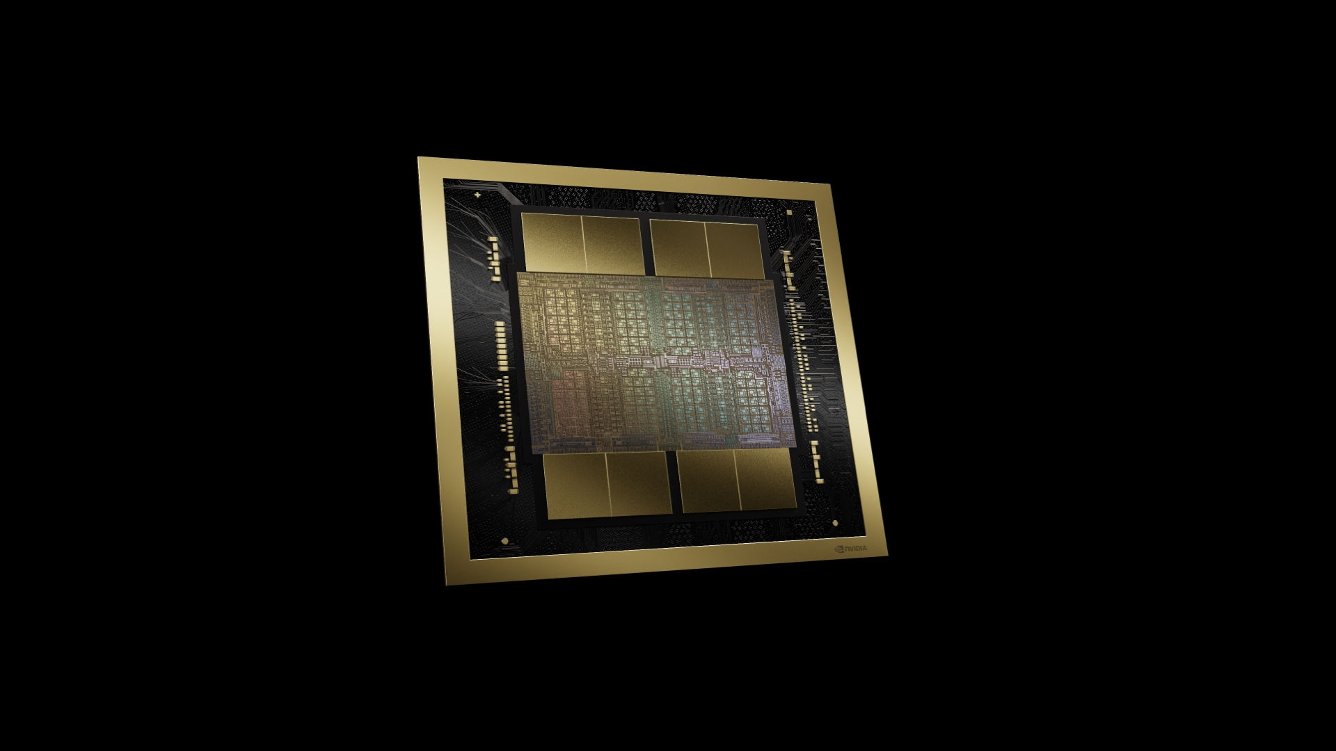
The AI factory era demands hardware that scales both compute and memory with high efficiency. NVIDIA’s Blackwell Ultra is described as the culmination of silicon innovations and system-level integration aimed at accelerating training and AI reasoning for large-scale, real-time AI services. The architecture relies on a dual-die design—two reticle-sized dies joined via NVIDIA High-Bandwidth Interface (NV-HBI)—to deliver a high-bandwidth, power-efficient data path (10 TB/s) between the dies, while remaining a CUDA-programmed accelerator that developers can leverage with familiar tooling. Blackwell Ultra is manufactured on TSMC 4NP and contains 208 billion transistors—about 2.6x more than the Hopper GPU—packaged as a single NVIDIA CUDA-programmed accelerator. The heart of the device comprises 160 SMs organized into eight Graphics Processing Clusters (GPCs). Each SM houses a dense compute capability designed to run modern AI workloads, including acceleration for attention operations that dominate modern transformer-based models.
What’s new
Blackwell Ultra introduces several architectural and capability advances aimed at raising throughput, reducing latency, and expanding memory headroom for the largest AI models:
- Fifth-generation Tensor Cores across all SMs, with a second-generation Transformer Engine, delivering higher throughput and lower latency for both dense and sparse AI workloads.
- Four Tensor Cores per SM (640 total) upgraded to handle NVFP4, the new 4-bit floating-point format.
- Each SM includes 256 KB of Tensor Memory (TMEM) to keep data close to compute units and supports dual-thread-block MMA, enabling paired SMs to cooperate on a single MMA operation and reduce memory traffic.
- NVFP4 precision combines FP8-like micro-block scaling (FP8 E4M3) with a tensor-level FP32 scale, enabling hardware-accelerated quantization with markedly lower error rates than standard FP4. NVFP4 offers near FP8-equivalent accuracy with substantially smaller memory footprints than FP16—benefiting low-precision AI inference.
- The base Blackwell architecture provides up to 10 petaFLOPS of NVFP4 performance; Blackwell Ultra pushes that to 15 petaFLOPS—a 1.5x uplift versus Blackwell and a 7.5x uplift versus Hopper/H100/H200 generations.
- Attention acceleration: SFU throughput for key attention instructions is doubled, delivering up to 2x faster attention-layer compute, mitigating latency bottlenecks in long-context transformer models.
- Memory capacity: Blackwell Ultra ships with 288 GB of HBM3e per GPU, representing 3.6x more on-package memory than H100 and 50% more than Blackwell, enabling trillion-parameter models and high-concurrency inference without frequent KV-cache offloading.
- Interconnect and host connectivity: Blackwell Ultra supports five-generation interconnects including NVLink for GPU-to-GPU, NVLink-C2C for coherent interconnect to an NVIDIA Grace CPU, and x16 PCI-Express Gen 6 for host communications, delivering a cohesive GPU-to-CPU-to-GPU data path.
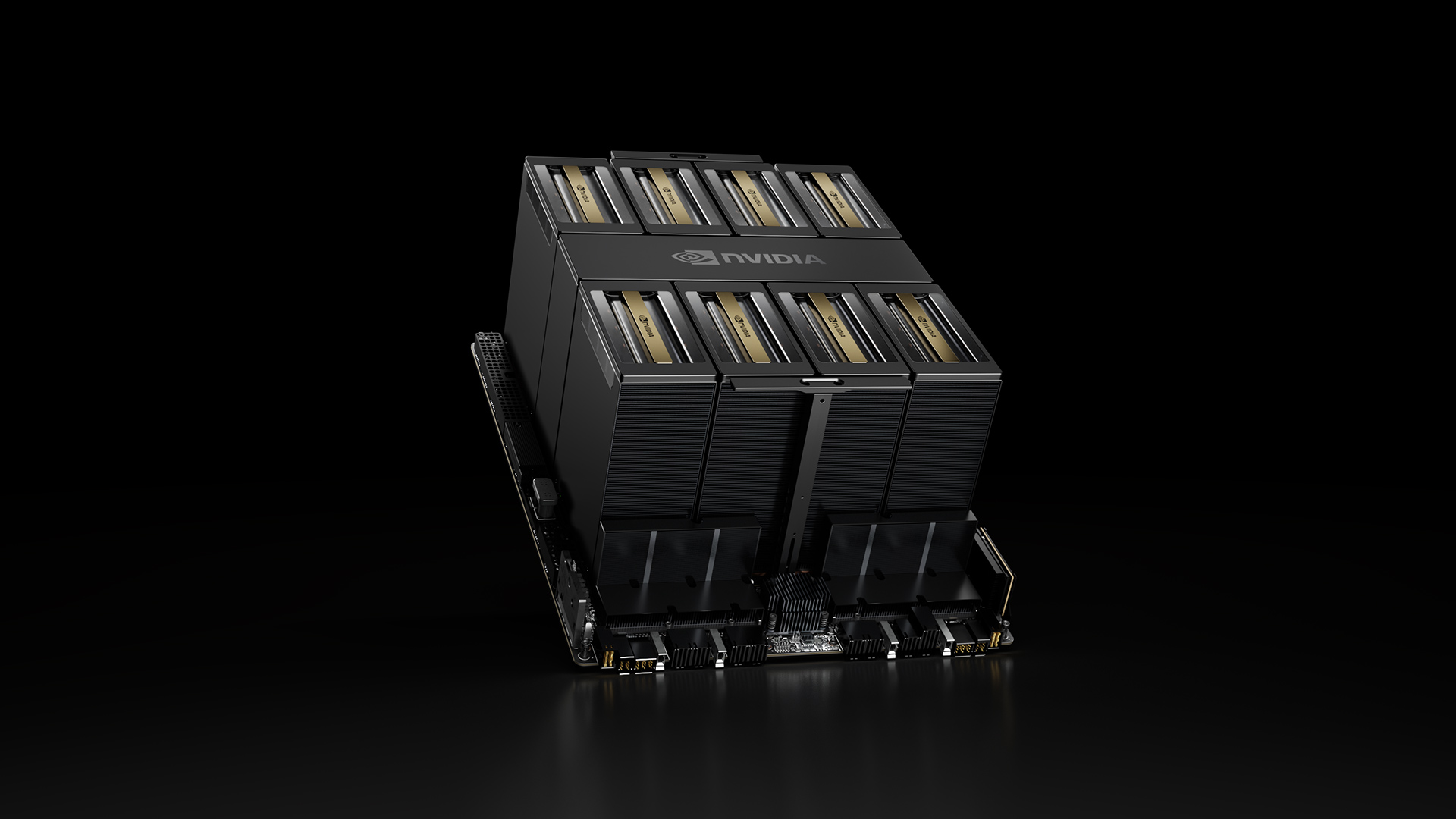
- System-level integration: The NVIDIA Grace Blackwell Ultra Superchip (GB300 NVL72 rack-scale system) pairs one Grace CPU with two Blackwell Ultra GPUs, delivering up to 30 PFLOPS dense and 40 PFLOPS sparse NVFP4 AI compute, with 1 TB unified memory (HBM3E + LPDDR5X) and 800 GB/s ConnectX-8 network connectivity.
Why it matters (impact for developers/enterprises)
Blackwell Ultra represents a step change in operational efficiency and raw AI throughput for production AI factories. The combination of higher memory density, higher precision-efficient compute, and doubled attention throughput translates into more model instances, faster responses, and lower costs per token generated in large-scale inference. The 288 GB HBM3e per GPU enables hosting trillion-parameter models and longer context windows without offloading data, while the enhanced interconnects and unified memory architecture improve end-to-end throughput from host to accelerators. For enterprises building AI services, the architecture aims to improve two key metrics:
- Tokens-per-second per user (TPS/user): accelerated softmax and attention processing reduce latency in real-time inference.
- Tokens-per-second per megawatt (TPS/MW): larger on-chip memory and efficient data movement raise data-center efficiency, enabling more work per watt.
Technical details or Implementation
The Blackwell Ultra design centers on dual-die integration via NV-HBI, delivering 10 TB/s bandwidth between the reticle-sized dies. The chip features 208B transistors on a TSMC 4NP process, enabling a compact yet highly dense compute engine that remains CUDA-programmable for easy software adoption. Key architectural elements include:
- 160 SMs organized into eight GPCs in the full GPU implementation.
- Each SM contains four Tensor Cores (640 total) upgraded for NVFP4 precision.
- 256 KB TMEM per SM, tightly integrated with the Tensor Cores to minimize data movement and maximize throughput.
- Dual-thread-block MMA: paired SMs cooperate on a single MMA operation, sharing operands and reducing redundant memory traffic.
- NVFP4 precision: a mixed FP8/FP32 scaling approach that achieves near FP8 accuracy with lower memory footprint than FP16 or FP32 norms, supporting efficient quantization for AI workloads.
- 15 petaFLOPS NVFP4 compute (Ultra) vs 10 petaFLOPS on the base Blackwell, marking a meaningful uplift in dense and sparse AI workloads.
- Attention acceleration: SFU throughput for key attention instructions is doubled, improving the efficiency of long-context transformer models.
- Memory footprint: 288 GB of HBM3e per GPU, 3.6x more than H100 and 50% more than Blackwell, addressing trillion-parameter models and extensive context lengths.
- Unified on-node memory: up to 1 TB of memory by combining HBM3E with LPDDR5X for large on-chip capacity.
- Interconnect and host connectivity: Blackwell Ultra supports NVLink for GPU-to-GPU communication, NVLink-C2C for Grace CPU coherence, and PCIe Gen 6 x16 for host connections; ConnectX-8 SuperNICs provide up to 800 GB/s network bandwidth.
- System-level deployment: in the Grace Blackwell Ultra Superchip (GB300 NVL72), a single Grace CPU connects to two Blackwell Ultra GPUs via NVLink-C2C, delivering up to 30 PFLOPS dense and 40 PFLOPS sparse NVFP4 AI compute. Table 1. Interconnects across generations (as described for Blackwell Ultra) | Interconnect | Description |--- |--- |NVLink | GPU-to-GPU communication over NVLink Switch |NVLink-C2C | Coherent interconnect to an NVIDIA Grace CPU |PCIe Gen 6 x16 | Interface for host CPUs | Table 2. (Referenced in NVIDIA materials) compares key chip specifications across Hopper, Blackwell, and Blackwell Ultra. The Ultra generation advances transistor count, memory capacity, interconnect bandwidth, and precision compute throughput, with architectural enhancements like attention acceleration and NVFP4.
Key takeaways
- Blackwell Ultra combines dual-die NV-HBI interconnect with a dense SM/RDMA compute fabric to push AI training and inference at factory scale.
- NVFP4 4-bit precision enables hardware-accelerated quantization with near FP8 accuracy and smaller memory footprints, benefiting large-scale inference.
- The architecture doubles attention-layer throughput and increases memory capacity to 288 GB HBM3e per GPU, enabling larger models and longer context windows.
- On-device TMEM and dual-thread-block MMA reduce memory traffic and improve sustained throughput for large-batch training and interactive inference.
- System-level integration, including NVLink, NVLink-C2C, PCIe Gen 6, and ConnectX-8 networking, supports scalable AI deployments from single GPUs to rack-scale AI factories.
FAQ
-
What is Blackwell Ultra designed to accelerate?
It is designed to accelerate training and AI reasoning for large-scale AI workloads and real-time AI services in data-center environments.
-
What is NVFP4 and why is it important?
NVFP4 is a new 4-bit floating-point format (with FP8 micro-block scaling and FP32 tensor-scale) that provides hardware-accelerated quantization with high accuracy and lower memory footprint, boosting efficiency for low-precision AI inference.
-
How much memory does Blackwell Ultra provide on-device?
It provides 288 GB of HBM3e per GPU, with a total on-node memory footprint of up to 1 TB when combined with LPDDR5X in the unified memory configuration.
-
What interconnects are supported for Blackwell Ultra?
NVLink for GPU-to-GPU, NVLink-C2C for Grace CPU coherence, and x16 PCI-Express Gen 6 for host connections, with 800 GB/s ConnectX-8 networking in system deployments.
-
How does Blackwell Ultra perform relative to prior NVIDIA generations?
It delivers up to 15 petaFLOPS NVFP4 compute (versus 10 petaFLOPS on Blackwell) and doubles certain attention SFU throughput, enabling faster, more efficient large-context AI workloads.
References
More news
NVIDIA HGX B200 Reduces Embodied Carbon Emissions Intensity
NVIDIA HGX B200 lowers embodied carbon intensity by 24% vs. HGX H100, while delivering higher AI performance and energy efficiency. This article reviews the PCF-backed improvements, new hardware features, and implications for developers and enterprises.

Predict Extreme Weather in Minutes Without a Supercomputer: Huge Ensembles (HENS)
NVIDIA and Berkeley Lab unveil Huge Ensembles (HENS), an open-source AI tool that forecasts low-likelihood, high-impact weather events using 27,000 years of data, with ready-to-run options.

Scaleway Joins Hugging Face Inference Providers for Serverless, Low-Latency Inference
Scaleway is now a supported Inference Provider on the Hugging Face Hub, enabling serverless inference directly on model pages with JS and Python SDKs. Access popular open-weight models and enjoy scalable, low-latency AI workflows.

How to Reduce KV Cache Bottlenecks with NVIDIA Dynamo
NVIDIA Dynamo offloads KV Cache from GPU memory to cost-efficient storage, enabling longer context windows, higher concurrency, and lower inference costs for large-scale LLMs and generative AI workloads.
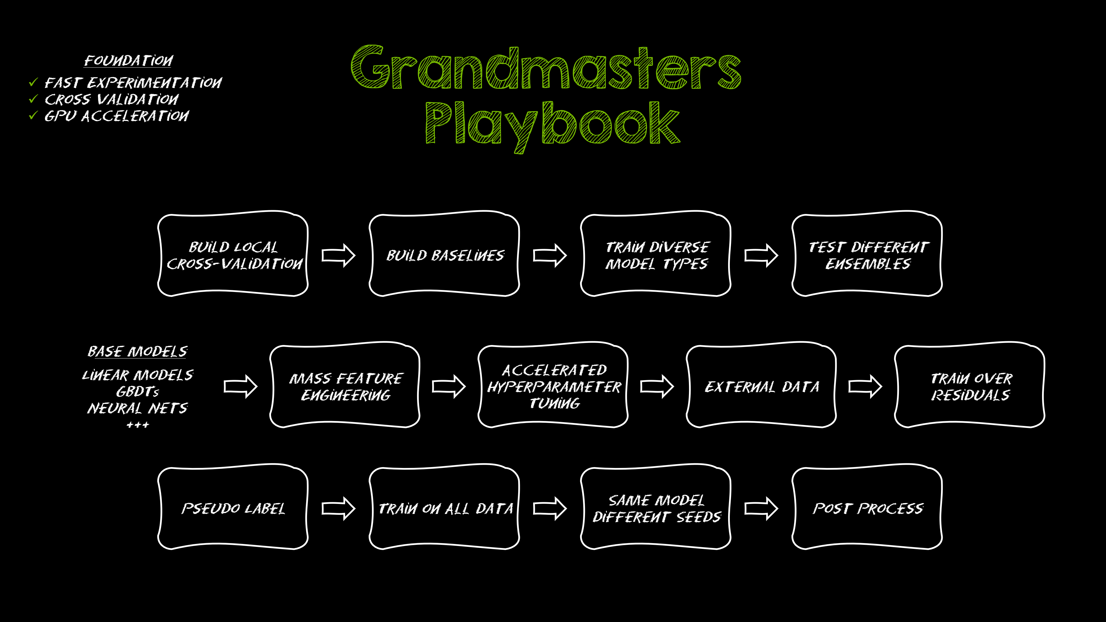
Kaggle Grandmasters Playbook: 7 Battle-Tested Techniques for Tabular Data Modeling
A detailed look at seven battle-tested techniques used by Kaggle Grandmasters to solve large tabular datasets fast with GPU acceleration, from diversified baselines to advanced ensembling and pseudo-labeling.
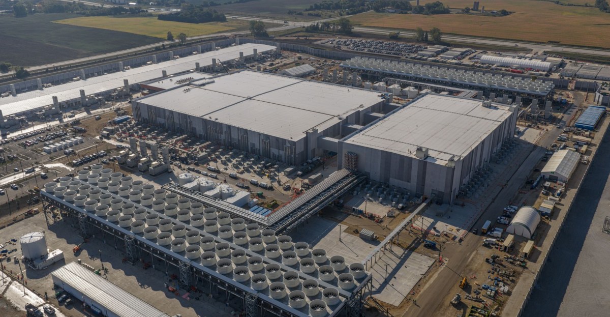
Microsoft to turn Foxconn site into Fairwater AI data center, touted as world's most powerful
Microsoft unveils plans for a 1.2 million-square-foot Fairwater AI data center in Wisconsin, housing hundreds of thousands of Nvidia GB200 GPUs. The project promises unprecedented AI training power with a closed-loop cooling system and a cost of $3.3 billion.